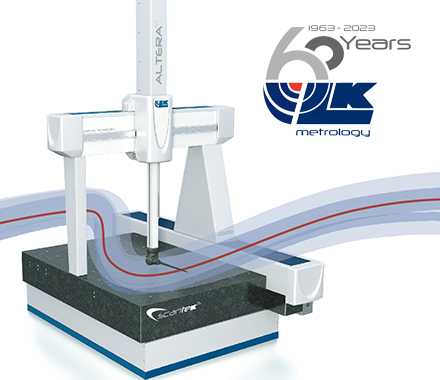
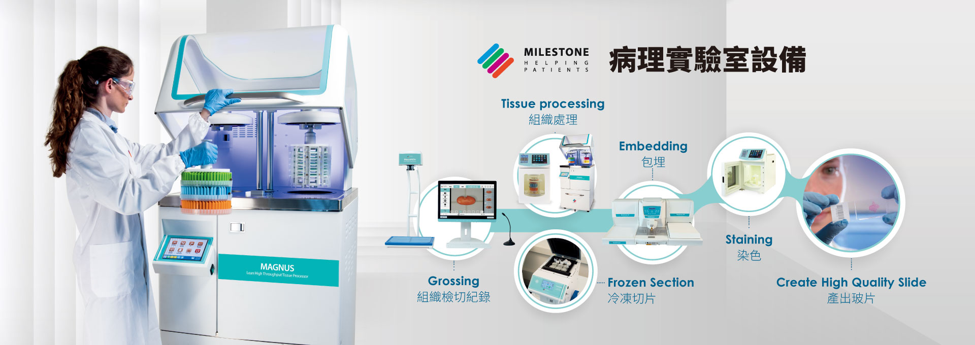
Zeiss MeRit
Requirements for Advanced Mask Repair
‧Support of small features sizes (< 65nm)
‧Low transmission loss
‧High resolution and non destructive defect review
‧Capability to support multiple processes
‧Support all future lithography approaches and mask materials (157nm, EUV, EPL, LEEPL, S-FIL)
‧High Throughput
Application Examples for Repair
The E-Beam Mask Repair System is capable to repair opaque and clear defects on photomasks. A deposition for missing material of a mousebite-defect in a line and spaces pattern is shown here:
The SEM image visualizes the lateral shape
The AFM image indicates the height profile
The AIMS image shows the feature printability onto the wafer, especially the VUV-transmission
For opaque defects, various etching process application modules are available, e.g. for Quartz, Chromium, Tantalum Nitride, Silicon Carbide, Molybdenum Silicide.
Benefits of E-Beam Mask Repair
‧Superior resolution and accuracy for repair
‧Repair process generates no transmission loss
‧No mask structure modification generated during imaging, allowing unlimited number of review cycles
‧End point definition through e-beam induced chemical reactions without any sputter contribution
‧High imaging signal-to-noise ratio results in better overall system performance
‧Multi-node capability
‧All-in-one-tool - high throughput
Principle of E- Beam Induced Chemical Reactions
Electron beam induced chemical reactions are exploited for etching and deposition of mask material. A suitable precursor gas is dispensed through a nozzle near to the focused electron beam. The precursor gas molecules adsorb at the substrate surface, and a reaction is induced by the electron beam. This reaction leads to either a deposition caused by fragmentation of precursor gas molecules or to an etching of the substrate material reacting into volatile products.
Mask Repair Software
‧Workflow oriented Graphical User Interface (GUI)
‧Seamless interface to most inspection system file
─- Mask alignment, defect navigation and characterization
‧End-point detection during etch by real-time monitoring of SE-signal
‧Extensive automation schemes:
─- setup and alignment (focus, stigmation, contrast, brightness)
─- edge detection and critical edge placement adjustment
─- drift monitoring and correction
─- Die-to-die pattern copy, defect pattern extraction, automatic pattern placement
‧Predefined processes for optimized deposition and etching
‧Customizable repair processes and applications
System Setup
The system is based on the robust, industry proven field emission scanning electron microscope with GEMINI electron optics, with a specific chamber, semi-automatic mask loader and a high precision laser interferometer stage. A combination of a electromagnetic and electrostatic final lens delivers ultra high resolution at low voltages, with a 3 nm spot size at 1 kV and a superior beam current of 20 nanoampere.
GEMINI principle
The hardware is completed by a proprietary five-channel gas injection system with gas cabinet housing the reservoirs and valve control. Furthermore, a dedicated e-beam scan generator is available for repair. Finally, special care had been taken to compensate for any mask charging by a proprietary method.
Technical Data
Lithography
248nm, 193nm , 157nm, EUV, EPL, LEEPL
Node
90nm / 65nm and beyond
Sample
6" mask
Repair Application
Chrome, TaN, MoSi, SiC, Si- etching,
Pt/C deposition, other materials upon request
Repair function
Polygon shape, Scan rotation, Pattern copy,
Real-time imaging of deposition and etching
Repair Accuracy
Currently 15nm @ 3 sigma (4 x mask),
target 7nm (pattern copy and placement function)
Minimum Repairable Defect
< 50nm
Resistance to chemicals
resistant to standard cleaning agents
Link with inspection tool
KLA file format, and others supported
Options
8" wafer capability, variable pressure chamber,
Loader adaptatio